Last
week Intel had their Q1 conference call for financial analysts, and
revealed that the 22-nm Ivy Bridge parts would make up 25% of their
shipment volume in the second quarter of this year. That means
that a good quantity will already will have shipped, and we managed to
track some down in Hong Kong a few weeks ago. Of course we got in
touch ASAP and the parts duly arrived, and they were the real thing.
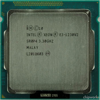 |
Fig. 1 Intel Xeon E3-1230V2 Server CPU |
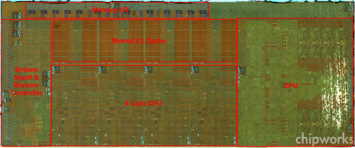
We
obtained samples of Xeon E3-1230 v2 CPUs, which are four-core, 3.3 GHz,
64-bit parts intended for the server market. Here is a die photo of
the transistor level, with annotations from
Intel's Ivy Bridge launch yesterday:
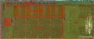 |
Fig.2 Intel Xeon E3-1230V2 Die |
A quick cross-section reveals that Intel have stayed with the nine metal layers used in the last two generations:
 |
Fig. 3 Intel Xeon E3-130V2 General Structure |
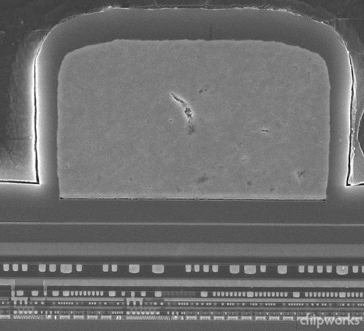
A
closer TEM image (Fig. 4) shows the lower metal stack and a pair of
multi-fin NMOS and PMOS transistors. This section is parallel to the
gate, across the fins, and we can see the contact trenches and metal
levels M1 up to M5.
We have to digress here a little to explain
what we’re looking at. A typical TEM sample is 80 – 100 nm thick,
to be thin enough to be transparent to the electron beam and at the same
time have enough physical rigidity so that it does not bend or fall
apart.
Here we are trying to image structures in a die with a
gate length of less than 30 nm; so if we make a sample parallel to the
gate, and if the sample is aligned perfectly along the centre of the
gate, then it will contain the gate plus at least part of the
source/drain (S/D) silicon and contacts on either side.
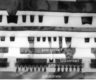 |
Fig. 4 TEM Image of Lower Metals and NMOS and PMOS (right) Transistors |
That
is what we see above – I have labeled the gate and contact stripes, and
we have PMOS on the right and NMOS on the left. The
tungsten-filled contacts obscure parts of the gate, but we can clearly
see that the PMOS S/D fins have epitaxial growth on them, and the fins
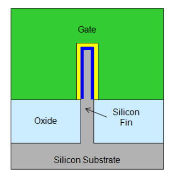
have an unexpected slope – a little different from Intel’s tri-gate
schematic shown last year –see Fig.5.
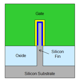 |
Fig. 5 Intel Schematic of Tri-Gate Transistor |
If
we zoom in a bit further into the PMOS gate (Fig. 6), we can see how
the gate wraps over the fin, and the rounded top of the fin. The
thin dark line adjacent to the fin is the high-k layer and just above
that is a mottled TiN layer that is likely the PMOS work-function
material, as in the 32-nm and 45-nm parts.
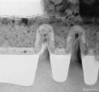 |
Fig. 6 TEM Image of PMOS Gate and Fin Structure |
Fig.
7 shows a section of an NMOS transistor. There is a ‘ghost’ of
the contact behind the gate, but the gate structure itself looks similar
to the PMOS, with the exception of the work-function material just
above the high-k layer (as expected).
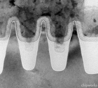 |
Fig. 7 TEM Image of NMOS Gate and Fin Structure |
Fig.
8 gives me an opportunity to show off our new TEM – we have recently
purchased an FEI Osiris machine, which upgrades our capability
considerably. Here we have a lattice image of a fin in an NMOS
transistor; the diamond-like layout of the pattern of dots is actually
created by the columns of atoms in the silicon crystal lattice. This
tells us that the sample is oriented in the <110> direction, which
given that silicon has a face-centred cubic structure in which
equivalent planes are at right angles, means that the channel direction
is also <110>.
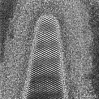 |
Fig. 8 TEM Lattice Image of NMOS Fin Structure |
To
fully understand what we’re looking at, of course, we need to see
what’s happening in the orthogonal direction, along the fin and
cross-sectioning the gate – as in Fig. 9. This shows an array of PMOS
transistors over a single fin, four functional gates and two dummy gates
at the ends of the fin. Again the TEM sample is thick compared with the
feature size, so we are seeing the gate on the side(s) of the fin, not
just the top. The fin ends have the same taper as in Figs 6 and 7.
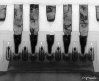 |
Fig. 9 TEM Image of PMOS Transistors |
As
announced by Intel, there is embedded SiGe in the source/drains,
although not etched to the <111> planes as in the 32- and 45-nm
product. It also looks as though the tops of the gates have been etched
back and back-filled with dielectric, and the contacts are self-aligned
as in memory chips.
Zooming in on the PMOS transistor in Fig.10,
the image is a bit fuzzy, but the SiGe is clearly in a rounded cavity
with no facets on the top, though there are facets on the sides of the
fin (see fig. 4).
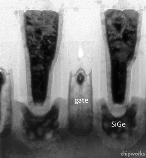 |
Fig. 10 TEM Image of PMOS Transistor |
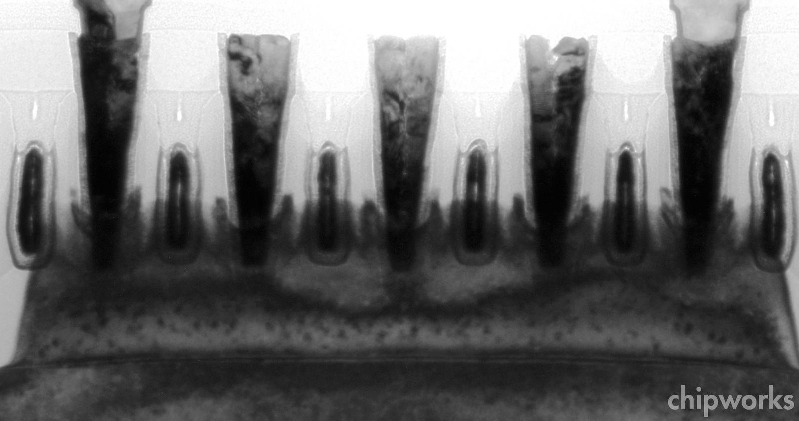
Looking
at the NMOS equivalent (Figs. 11 and 12), we see a similar structure –
there seems to be an epitaxial interface, and the silicide(?) seems to
protrude slightly above the fin.
 |
Fig. 11 TEM Image of NMOS Transistors |
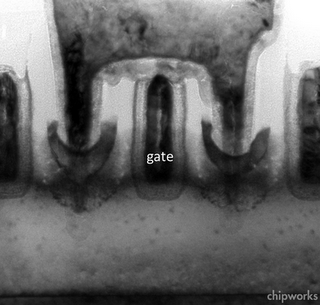 |
Fig. 12 TEM Image of NMOS Transistors |
It
is hard to say much about the gates here, either NMOS or PMOS, because
of the sample thickness problem; we are viewing a slice that includes
the gate on both sides of the fin and the fin itself. Fortunately we
have images of gate metal over STI and they are less confusing.
Figure
13 is a composite image of NMOS and PMOS gates so that the differences
are highlighted. The dark line surrounding the gate structures is the
Hf-based high-k, and within that are the two work-function materials,
likely TiN for PMOS and TiAlN for NMOS. (The columnar structure of the
PMOS TiN is visible in the right half of the image.)
 |
Fig. 13 Composite TEM Image of NMOS/PMOS Gates |
The
fill has been changed from TiAl in the earlier parts to tungsten. It is
more prominent in the NMOS gates than the PMOS, because the PMOS
structure includes both work-function metals, whereas the TiN has been
etched out of the NMOS gates. At the 45-nm node Intel used tensile
tungsten in the contacts to apply channel stress – have they transposed
this to the gates in the 22-nm process?
Just to finish up, so
that this is still a blog, not a paper (I don’t want to go on too long) –
fig. 14 shows a sample delayered to expose the transistors, and imaged
on a tilt angle. Both the gates and the fins show up nicely, and
we can actually see tiny spikes of SiGe in the PMOS source/drains. The
small pillars in between the fins in the NMOS areas are residual bits of
contact metal. I think it’s a cool image!
 |
Fig. 14 Tilt SEM Image of NMOS/PMOS Transistors |
We are just getting into the full scope of the
analysis, so likely more to come in the next few weeks!
I'm still tweeting as @ChipworksDick, for those that way inclined..